- Lithography
- Physical Vapor Depostion
- Chemical Vapor Deposition
- Dry Etching
- Wet Benches
- Anealing
- Wafer Bonding Sawing and Packaging
- Direct Writing
- Characterization
Lithography
Instruments:
UV Aligner | Mask Aligner | Spray Coater
Edge Bead Remover | Manual Spin Coat Station
Spin Coater 2 | Hot Plate
UV Aligner
Make & Model: EVG 620 (Year 2002)
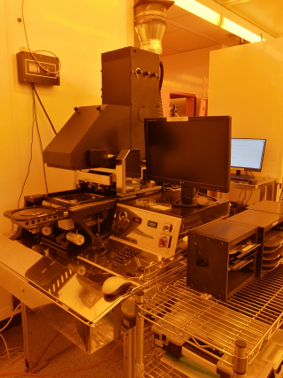
Specifications:
- 6 inch compatible aligner. Down 0.8um in resolution 1um topside alignment
- 5 exposure modes: vacuum contact, vacuum hard, hard contact, soft contact, and proximity
- frontside and backside alignment
- objectives available: 10X, 20X, 50X, and flat objective (for pieces)
- bonding chucks for anodic bonding, thermal compression bonding and fusion bonding.
- 2" chuck can be used for 2" wafers and pieces as well
- minimum resolution in dark field = 0.7 µm line and <1 µm contacts
- minimum resolution in clear field = 2 µm line and 2 µm contacts
- 2", 4" and 6" wafers, 3", 5" and 7" masks
- max wafer thickness 4.6 mm
Mask Aligner
Make & Model: SUSS MA/BA6 Gen 4

Specifications:
- Exposure Wavelengths:
- g-line (436 nm).
- h-line (405 nm).
- i-line (365 nm).
- UV Broadband (350 nm to 450 nm).
- Illumination area: 150 mm diameter.
- Resolution: 1 µm.
- Frontside and Backside Alignment.
- Top Side Overlay accuracy: 500 nm.
- Backside Overlay accuracy: 1000 nm
Spray Coater
Make & Model: EVG 101

Specifications:
- Wafer size up to 300 mm
- Automated spin or spray coating or developing with manual wafer load/unload
- Quick and easy process transfer from research to production utilizing proven modular design and standardized software
- Syringe dispense system for utilization of small resist volumes, including high-viscosity resists
- Small footprint while maintaining a high level of personal and process safety
- Multi-user concept (unlimited number of user accounts and recipes, assignable access rights, different user interface languages)
Options:
- Uniform coating of high-topography wafer surfaces with OmniSpray® coating technology
- Wax and epoxy coating for subsequent bonding processes
- Spin-On-Glass (SOG)
Edge Bead Remover
Make & Model: Laurell Technologies

Manual Spin Coat Station
Make & Model: Laurell WS-400B-6NPP/LITE
Specifications:
Manual tabletop spinner with vacuum check and nitrogen purge, mainly for spin photoresists, support upto 6 inch wafer.
Spin Coater 2
Make & Model: MicroNanotools KW-4A

Specifications:
Manual coater for PDMS and polyimide material, up to 6 inch wafer
Hot Plate
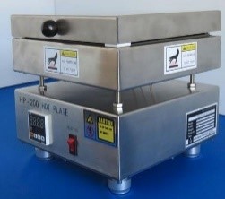
Applications:
Soft and hard baking photoresist
Physical Vapor Deposition
Instruments:
Sputter | Ebeam Evap1 | Ebeam Evap2
Sputter
Make & Model: Denton E14

Specifications & Applications:
- Denton Vacuum Explorer 14 Sputtering System is used to deposit the thin films of dielectric material or metals by using magnetron gun
- It supports up to 6 inch wafer, two DC, one RF, heated stage up to 250 °C
Make & Model: Angstrom Engineering AMOD

Specifications & Applications:
- RF, DC, pulsed DC, HIPIMS, and reactive
- Materials: SiO₂, SiN, ITO, Ti, Cr, Mo, Zr, Au, Al, SiC...
Ebeam Evap 1
Make & Model: BJD 1800

Specifications & Applications:
- The model BJD-1800 (Al) provides thin film coating of virtually any material quickly, cleanly and efficiently.
- Our system is equipped with 10 kW e-Gun power supply, 4 pocket material source, thickness monitoring, sample heater, and indirect temperature monitoring.
- A variety of evaporation source materials are available.
- A base pressure in the system is 2 x 10⁻⁷ Torr.
- The vacuum recommended for deposition is 2 x 10⁻⁶ Torr or better.
- Planar and planetary rotatable sample holders are available.
Ebeam Evap 2
Make & Model: Angstrom Scientific Nexdep

Specifications & Applications:
- The NexDep evaporator equipped with a 6-pocket gun and a 10kW power supply.
- 6 pocket material source, thickness monitoring, sample heater, up to 6 inch wafer
- Material available are Au, Ti, Cr, Pd, Pt, Cu, NiFe, Ni, Al ...
Chemical Vapor Deposition
Instruments:
PECVD | Atomic Layer Deposition System | Parylene Coater
PEVCD
Make & Model: Applied Material P5000

Specifications and Applications:
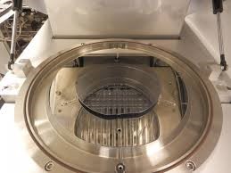
- P5000 is a load-locked, magnetically enhanced reactive ion etching system (MERIE) with 4l process chambers (ChambersA, B,C&D).
- P5000 Chamber A is mainly used for metal etching
- Chamber B is primarily used for etching silicon based dielectrics (silicon dioxide, silcon nitride, etc.) and some carbon based compounds (resist, poly imide, etc)
- Chamber C is mainly uused for silicon etching with high slectivity to underlying dielectric such as silicon dioxide
- Chember D is PECVD, mainly for dielectric deposition such as SiN and PolySi. The system can process only 6" wafers.
- Though the process chamber processes one at a time, upto 25 wafers can be loaded per batch.
Atomic Layer Deposition (ALD)
Make & Model: Veeco Fiji G2

Specifications & Applications:
The Fiji G2 is a next-generation ALD system capable of performing thermal and plasma-enhanced deposition.
- Materials: TiO₂, Al2O3, SiO₂, HfO₂
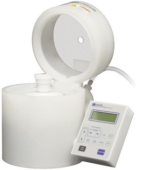
Parylene Coater
Make & Model: Specialty Coating Systems SCS 200

Specifications & Applications:
Parylene coating system, C, D, N, 10 nm to 8 um
Dry Etching
Instruments:
Xenon Difluoride Etcher | High Density Plasma Treatment System | DRIE | RIE | ICP
Xenon Difluoride Etcher
Make & Model: Xactix E2
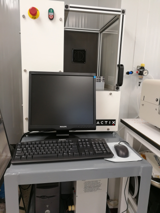
Specifications & Applications:
- The XACTIX XeF2 etching system is an isotropic silicon etching system.
- XeF2 etching is a dry, room temperature process. It is particularly well suited to MEMS applications.
- This system can provide nearly infinite selectivity of silicon to photoresist, SiO2, Si3N4, Al, and Cr.
- The system process chamber can accommodate individual die, pieces of wafer, and full wafers up to 6” in diameter.
- The recipe-driven control software will manage multiple users and log all process data.
High Density Plasma Treatment System
Make & Model: Nanoplas Model DSB 600

Specifications & Applications:
- Advanced plasma cleaning for 150mm Features Batch processing of up to 25 wafers (150mm)
- Single-wafer processing up to 200mm Single-wafer stage heating up to 250°C
- Heated quartz chamber up to 180°C 600W ICP source (13.56MHz)
- External vacuum pump PLC control with touch-screen interface, primarily made to strip, descum photoresist and remove polymers deposited during other Plasma etching processes
DRIE
Make & Model: Oxford Instrument Plasma Pro 100 Estrelas

Specifications & Applications:
- Chemical: O₂, Ar, SF₆, C4F8
- Application: High-aspect-ratio etching for MEMS and other applications
RIE
Make & Model: Applied Materials AM5000
Specifications & Applications:
-
Chemical: Cl₂, CF₄, CHF₃, SF₆, O₂, Ar
-
Application: Versatile plasma etching for various materials
ICP
Make & Model: PlasmaTherm APEX SLR

Specifications & Applications:
The Plasma-Therm Apex SLR is a High Density Plasma Chemical Vapor Deposition (HDPCVD) system. It uses an Inductively Coupled Plasma (ICP) source to generate higher density plasma than a PECVD system providing deposition at lower temperatures for higher quality, low temperature films.
- 1 kW 2 MHz ICP source
- 300 W, 13.56 MHz electrode
- 254 mm plate
- Low temperature deposition, typically 80 ° - 150 °C
- Liquid-to-liquid heat exchanger
- Compatible with film etching for SiNx, SiO2, a-Si, SiOxNy, SiC, Ta2O5.
- Compatible with film etching for polymers such as photoresist and polyimide
- Endpoint Detection
- ANSI-ISA 88 data logging and recipe management
Wet Bench
Instruments:
Si Etch Wetbench | Acid Wetbench| HF Wetbench | Solvent Wetbench | Litho Wetbench
Si Etch Wetbench (Base Wetbench)
Make & Model: SIC Wetbench

Applications:
The wet bench is specifically for base process, mainly for TMAH and KOH based Silicon etching
Acid Wetbench
Make & Model: SIC Wetbench

Applications:
The acid bench for sample cleaning, metal etching
HF Wetbench
Make & Model: Reynold

Applications:
Wet bench, specifically for HF etching
Solvent Wetbench
Make & Model: SIC Solvent Wetbench

Applications:
Wet bench for sample cleaning, stripping, lift-off and PR development.
Litho Wetbench
Make & Model: SIC Litho Wetbench

Applications:
Wetbench for general sample cleaning, PR development
Annealing
Instrument: Rapid Thermal Annealing
Rapid Thermal Annealing
Make & Model: Qualiflow Jetfirst


Specifications:
- RTP processor for wafers up to 8 " wafer
- Temperature range: ambient to 1300 °C
- Ramp rate: 1°C/s to 300 °C/s
- Gases available: N2, H2/N2 (forming gas), O2, Ar
Wafers Bonding Sawing and Packaging
Instruments:
Wafer Bonder | Dicing Saw | Wire Bonder
Wafer Bonder
Make & Model: EVG 501
 Specifications:
6inch wafer bonder for anodic, direct and eutectic bonding.
Dicing Saw
Make & Model: Disco DAD3240
Specifications:
- Up to 6inch wafers
- Automatic control
- Glass and silicon blade
Wire Bonder
Make & Model: WestBond 747677E
Specifications:
Manual ultrasonic wedge wire bonder
Direct Writing
Instruments:
Laser Writer | Nano Frazor | Electron Beam Litho
Laser Writer
Make & Model: Kloe Dilase 650

Specifications & Applications:
- The High resolution direct laser lithography system Dilase 650 offers you the possibility to work with one or two writing lasers, to be focused into one to two beam sizes ranging from 1µm to 50 µm.
- It allows the writing on any type of substrate (photomasks, semiconductors, glass, polymers, crystals, flexible films...) over a surface area as large as 6 inches
Nano Frazor
Make & Model: Heidelberg Explorer

Specifications:
- Thermal Scanning Probe cantilevers with ultra-sharp tips
- 3D nanolithography
- In-situ metrology with sub-nm resolution for overlay, stitching & closed-loop lithography
- Real-time, automatic tuning of patterning parameters
- Short overall fabrication time, no resist development needed
- Stand-alone unit with low requirements on infrastructure (no vacuum or high voltages required)
- High degree of customization and automatization
- Ideal for small workpieces up to a size of 4-inch
- Compatibility with various transfer processes and materials
- Exchange and calibration of cantilevers within one minute
Electron Beam Litho
Make & Model: Tescan MIRA3 XMH

Specifications:
1.2nm resolution at 30KV, with NPGS software
Characterization
Instruments:
SEM | Optical Profiler | Optical Microscope | Reflectometer | Profilometer
SEM
Make & Model: Tescan VEGA 3 XMH

Specifications:
- High vacuum chamber
- Accelerating voltage: 200V – 30KV
- Best resolution: 2nm at 30kV
Applcations:
This SEM is for imaging and characterization of the samples
Optical Profiler
Make & Model: Wyko NT8000

Specifications:
- Optical profiler, with 8mm scan length
- 5x and 50x objectives
- 8" programmable stage
- LED illumination system
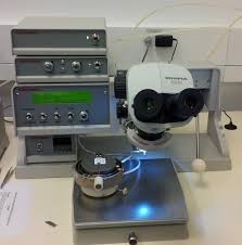
Optical Microscope
Make & Model: Olympus MX51

Specifications:
Sample inspection, 5x, 10x, 20x, 50x
Reflectometer
Make & Model: Filmetrix F10-RT

Specifications:
- Thickness range:15nm-70um
- Wavelength range: 380-1050nm
Make & Model: NanoSpec 6100

Specifications:
- Measures thin film thickness and optical properties based on reflectance.
Profilometer
Make & Model: Ambios XP200
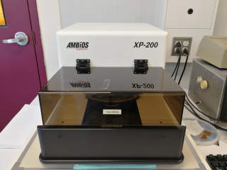
Specifications:
- Height range upto 800um
- Scan length upto 55mm support 200mm wafer with vacuum
Applications:
- A stylus scans the sample surface at a programmable speed, while its position is sampled at small and regular intervals
- The data is logged and then processed by the application software to extract useful information such as step height, surface roughness and waviness