Booking other characterization equipment
- SEM
- Ellipsometer
- Optical Profiler
- Optical Microscope
- Reflectometer
- Profilometer
- Stress Measurement
Would you like to receive the MIAM newsletter and be notified of future MIAM events?
Characterization Equipment
XPS
X-ray Photoelectron Spectroscopy (XPS): Thermo Fisher-Scientific Nexsa G2

Specifications:
- X-ray source: Al Kα micro-focused monochromator; spot size (10-400 μm)
- Analyzer: 180° double focusing hemispherical analyzer; 128-channel detector
- Charge compensation: dual beam source; ultra-low energy electron beam
- MAGCIS ion gun: monatomic mode: 500eV – 4keV; cluster mode: 2keV – 8keV, atom size: 75 – 2000
- Sample handling: 60×60mm sample area; 20mm maximum sample thickness
- Data system: Avantage data system
Applications:
- Surface characterization for a variety of solid materials: metals, oxides, polymers, semiconductors, microelectronics, nano and bio-materials
- No special preparation required for powders, fibers, coatings, films, bulk materials
- Element identification with the detection limit of 0.05%
- Chemical state (bond) analysis with high resolution scanning
- Depth profile performed either with monoatomic or cluster ion Ar gun
- Integrated analysis options:
- Ultraviolet photoelectron spectroscopy (UPS)
- Investigation of valence band and highest molecular orbitals (occupied bonding states)
- Work function measurements of materials
- Ion scattering spectroscopy (ISS)
- Elemental composition (except H) of the 1st atomic layer of a surface
- Reflection electron energy loss spectroscopy (REELS)
- Relative energy levels of unoccupied States.
- Band gap determination for semiconductor materials.
- Comparison of relative hydrogen content in polymer materials.
- Investigation of conjugation or aromaticity in organic materials.
- Determination of sp2 / sp3 hybridisation of carbon
- Rapid XPS imaging
- Tilt module for angle resolved XPS (ARXPS)
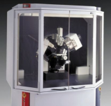
XRD 2
Bruker X-ray Diffraction (XRD) Analysis: D8 DISCOVER

Specifications:
- High-performance Cu X-ray sources
- X-ray Optics: monochromatic
- Goniometer and Sample Stage: XYZ, 1/4-Cradle
- Sample Alignment and Monitor: Optical/video microscope, laser/video
- 2D Detector: VANTEC-2000, the largest 2Theta and Gamma coverage
Applications:
- Enables detailed analysis of any crystalline materials from fundamental research
- Phase identification (Qualitative / Quantitative Analysis)
- Crystal structure determination / Crystalline percentage
- Grazing Incident X-Ray Diffraction (GIXRD)
- Various solid materials in the forms of powder, bulk and film samples
Confocal Raman/fluorescence microscope
Bruker Senterra Confocal Raman Microscope

Specifications:
- System: Bruker Senterra Dispersive Raman
- Detector Model: DU420A-OE-152
- Lasers: 785, 633 and 532 nm
- Microscope: Olympus BX51M System Metallurgical Microscope with halogen light source
- Software: OPUS 6.5.97; DSD 6.5.92.7101
Applications:
- Analyzes a vast range of samples, including biological samples.
- A special hardware feature removes fluorescence background at 785 nm.
- Sample maps with ~1 micron resolution can be obtained with a computer controlled sample stage, and polarizers and analyzers allow user to take polarized spectra.
- Can measure fluorescence maps using the Olympus optical microscope installed on the instrument.
- Connection with the MultiRAM to measure spectra with excitation wavelength of 1064 nm.
Bruker High Resolution Micro-Computed Tomography (microCT): Skysan1172
SEM
Tescan VEGA 3 XMH
Specifications:
- High vacuum chamber
- Accelerating voltage: 200V – 30KV
- Best resolution: 2nm at 30kV
Applcations:
- This SEM is for imaging and characterization of the samples
Optical Profiler
Wyto NT8000

Specifications:
- Optical profiler, with 8mm scan length
- 5x and 50x objectives
- 8" programmable stage
- LED illumination system
Optical Microscope
Olympus MX51

Specification and Application:
- Sample inspection, 5x, 10x, 20x, 50x
Reflectometer
Filmetrix F10-RT

Specifications:
- Thickness range:15nm-70um
- Wavelength range: 380-1050nm
Profilometer
Ambios XP200
Specifications:
- Height range upto 800um
- Scan length upto 55mm support 200mm wafer with vacuum.
Applications:
- A stylus scans the sample surface at a programmable speed, while its position is sampled at small and regular intervals.
- The data is logged and then processed by the application software to extract useful information such as step height, surface roughness and waviness.
Stress Measurement
Flexus 5200

Specifications and Applications:
- The Flexus 5200 Film stress meter system calculates film stresses.
- It optically measures a wafer curvature radius with and without the deposited film; knowing the wafer thickness, the film thickness and the wafer modulus, Stoney's equation yields the film stress.
Back to top


