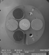
MicroCT
Make & Model: Bruker High Resolution Micro-Computed Tomography (microCT): Skysan1172
![]()
![]()


Instrument:
- X-ray source: 20-100kV,10W, <5 µm spot size
- Detail detectability: 0.5 µm at highest resolution
- X-ray detector: 11Mp, 12-bit cooled CCD fiber-optically coupled to scintillator
- Maximum object size: 27mm in diameter (single scan) or 50mm in diameter (offset scan)
- Continuous scanning for long objects with 70mm maximum in length
Applications:
- Used for life science research, clinical research, material research (metals, polymers & plastics, ceramics, composites, etc.)
- Allow to cut virtual sections or even fly through samples non-destructively
- 2D/3D image analysis and realistic visualization of an object's internal microstructure - microtomography or micro-CT
- No special preparation, coating or vacuum treatment is needed for samples
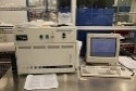
XRD 2
Make & Model: Bruker X-ray Diffraction (XRD) Analysis: D8 DISCOVER


Instrument:
- High-performance Cu X-ray sources
- X-ray Optics: monochromatic
- Goniometer and Sample Stage: XYZ, 1/4-Cradle
- Sample Alignment and Monitor: Optical/video microscope, laser/video
- 2D Detector: VANTEC-2000, the largest 2Theta and Gamma coverage
Applications:
- Enables detailed analysis of any crystalline materials from fundamental research
- Phase identification (Qualitative / Quantitative Analysis)
- Crystal structure determination / Crystalline percentage
- Grazing Incident X-Ray Diffraction (GIXRD)
- Various solid materials in the forms of powder, bulk and film samples
XPS
Make & Model: X-ray Photoelectron Spectroscopy (XPS): Thermo-Scientific K-Alpha


Instrument:
- X-ray source: Al Kα micro-focused monochromator; Spot size (30-400 μm)
- Analyzer: 180° double focusing hemispherical analyzer; 128-channel detector
- Charge Compensation: Dual beam source; Ultra-low energy electron beam
- Ion Gun: Energy range 200eV – 3keV
- Sample Handling: 60×60mm sample area; 20mm maximum sample thickness
- Vacuum System: 2 turbomolecular pumps for entry and analysis chambers
- Data System: Avantage data system
Applications:
- Surface characterization for a variety of solid materials: metals, oxides, plastics, polymers, semiconductor and microelectronics, nano-engineering, and bio-materials
- No special preparation required for various forms: powders, fibers, coatings, films, bulk materials
- Element identification with the detection limit of 0.05%
- Chemical state (bond) analysis with high resolution scanning
- Depth profile analysis with Ar Ion gun sputtering
- Tilt module for Angle reserved XPS (ARXPS)
SEM
Make & Model: Tescan VEGA 3 XMH

This SEM is for imaging and characterization of the samples. High vacuum chamber, accelerating voltage; 200V – 30KV, best resolution: 2nm at 30kV
Ellipsometer
Make & Model: Spora GES-5E

GES5E Optical Platform allows various measurement modes from Standard Ellipsometry to generalized Ellipsometry going thru photometric measurements (in Transmission and Reflection), Scatterometry, luminescence measurements. All measurements are made automatically as a function of: wavelength, angle of incidence, polarization state and time. Standard spectral range is 230-900 nm
Optical Profiler
Make & Model: Wyto NT8000

Optical profiler, with 8mm scan length
- 5x and 50x objectives
- 8" programmable stage
- LED illumination system
Optical Microscope

Reflectometer
Make & Model: Filmetrix F10-RT

Thickness range; 15nm-70um wavelength range: 380-1050nm
Profilometer
Make & Model: Ambios XP200

A stylus scans the sample surface at a programmable speed, while its position is sampled at small and regular intervals. The data is logged and then processed by the application software to extract useful information such as step height, surface roughness and waviness. Height range upto 800um, scan length upto 55mm support 200mm wafer with vacuum.
Stress Measurement
Make & Model: Flexus 5200
The Flexus 5200 Film stress meter system calculates film stresses. It optically measures a wafer curvature radius with and without the deposited film; knowing the wafer thickness, the film thickness and the wafer modulus, Stoney's equation yields the film stress.