- Lithography
- Physical Vapor Deposition
- Chemical Vpor Deposition
- Dry Etching
- Wet Benches
- Annealing and Oxidation
- Wafers Bonding Sawing and Packaging
- Direct Writing
- Other
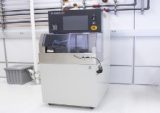
Lithography
UV Aligner 1
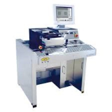
Make & Model: EVG 620 (Year 2002)
6 inch compatible aligner. Down 0.8um in resolution 1um topside alignment
- 5 exposure modes: vacuum contact, vacuum hard, hard contact, soft contact, and proximity
- frontside and backside alignment
- objectives available: 10X, 20X, 50X, and flat objective (for pieces)
- bonding chucks for anodic bonding, thermal compression bonding and fusion bonding.
- 2" chuck can be used for 2" wafers and pieces as well
- minimum resolution in dark field = 0.7 µm line and <1 µm contacts
- minimum resolution in clear field = 2 µm line and 2 µm contacts
- 2", 4" and 6" wafers, 3", 5" and 7" masks
- max wafer thickness 4.6 mm
UV Aligner 2
Make & Model: EVG 620 (Year 2018)
- Interchangeable mask frame and bond tools permit alignment of mask-to-wafer or wafer-to-wafer.
- Frontside mask-to-wafer alignment accuracy to <0.6 microns.
- Precision front-to-backside alignment to < 1 micron.
- Four different mask exposure modes: proximity, soft- and hard- contact, and vacuum contact.
- Fully motorized, split field microscopes with multiple objectives for wafer top and bottom side viewing.
- Backside alignment modes: optical image capture, user-specified cross-hairs, or customized alignment keys.
- Near UV (350 - 450 nm) lamp source.
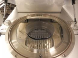
Develop Station

Make & Model: Laurell WS-1000MH/EDC-650-8NPP
Developing station for wafers (2, 3, 4 and 6 inches) and photomasks (3, 5 and 7 inches) Developers available: MF-319, AZ 400K, AZ 726 MIF, AZ 300
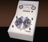
Spray Coater

Make & Model: EVG 101
- Wafer size up to 300 mm
- Automated spin or spray coating or developing with manual wafer load/unload
- Quick and easy process transfer from research to production utilizing proven modular design and standardized software
- Syringe dispense system for utilization of small resist volumes, including high-viscosity resists
- Small footprint while maintaining a high level of personal and process safety
- Multi-user concept (unlimited number of user accounts and recipes, assignable access rights, different user interface languages)
- Options:
- Uniform coating of high-topography wafer surfaces with OmniSpray® coating technology
- Wax and epoxy coating for subsequent bonding processes
- Spin-On-Glass (SOG)
Manual Spin Coat Station
Make & Model: Laurell WS-400B-6NPP/LITE
Manual tabletop spinner with vacuum check and nitrogen purge, mainly for spin photoresists, support upto 6 inch wafer.
Spin Coater 2
Make & Model: MicroNanotools KW-4A
Manual coater for PDMS and polyimide material
Covection Oven
Make & Model: Fisher BlueM
18.4L capacity, up to 250C, digital control
Priming Oven

Make & Model: YES-310E
YES Vacuum Convection Oven can be used to cure polyimide films on only Silicon and quarts/glass substrates in an O2 and H2O free environment and HDMS coating. Any other substrate or materials must be approved by the staff before use. Chamber temp is 20C -300C
Physical Vapor Deposition
Sputter

Make & Model: Denton E14
Denton Vacuum Explorer 14 Sputtering System is used to deposit the thin films of dielectric material or metals by using magnetron gun, support up to 6 inch wafer, two DC, one RF, heated
Ebeam Evap1
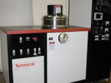
Make & Model: BJD 1800
The model BJD-1800 (Al) provides thin film coating of virtually any material quickly, cleanly and efficiently. Our system is equipped with 10 kW e-Gun power supply, 4 pocket material source, thickness monitoring, sample heater, and indirect temperature monitoring. A variety of evaporation source materials are available. A base pressure in the system is 2 x 10⁻⁷ Torr. The vacuum recommended for deposition is 2 x 10⁻⁶ Torr or better. Planar and planetary rotatable sample holders are available.
Ebeam Evap2

Make & Model: Angstrom Scientific Nexdep
The NexDep evaporator equipped with a 6-pocket gun and a 10kW power supply. Material available are Au, Ti, Cr, Pd, Pt, Cu, NiFe, Ni, Al ...
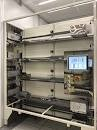
Chemical Vapor Deposition
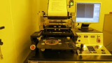
RIE/PECVD

Make & Model: Applied Material P5000
P5000 is a load-locked, magnetically enhanced reactive ion etching system (MERIE) with 4l process chambers (ChambersA, B,C&D). P5000 Chamber is A is mainly used for metal etching, Chamber B is primarily used for etching silicon based dielectrics (silicon dioxide, silcon nitride, etc.) and some carbon based compounds (resist, poly imide, etc) while chamber C is mainly uused for silicon etching with high slectivity to underlying dielectric such as silicon dioxide. Chember D is PECVD, mainly for dielectric deposition such as SiN and PolySi. The system can process only 6" wafers. Though the process chamber processes one at a time, upto 25 wafers can be loaded per batch.
Atomic Layer Deposition System (ALD)
Make & Model: Arradiance Gemstar8 ALD
GEMStar ALD systems deposit metal, semiconductor and insulating films, support 6 inch wafer, up to 6 wafers a batch
Processes Available
- thermal Aluminum oxide
- thermal Titanium oxide
- thermal Silicon oxide
- thermal Hafnium oxide
Dry Etching
Xenon Difluoride Etcher
Make & Model: Xactix E2
The XACTIX XeF2 etching system is an isotropic silicon etching system. XeF2 etching is a dry, room temperature process. It is particularly well suited to MEMS applications. This system can provide nearly infinite selectivity of silicon to photoresist, SiO2, Si3N4, Al, and Cr. The system process chamber can accommodate individual die, pieces of wafer, and full wafers up to 6” in diameter. The recipe-driven control software will manage multiple users and log all process data.
High Density Plasma Treatment system

Make & Model: Nanoplas Model DSB 600
Advanced plasma cleaning for 150mm Features Batch processing of up to 25 wafers (150mm) Single-wafer processing up to 200mm Single-wafer stage heating up to 250°C Heated quartz chamber up to 180°C 600W ICP source (13.56MHz) External vacuum pump PLC control with touch-screen interface, primarily made to strip, descum photoresist and remove polymers deposited during other Plasma etching processes
DRIE
Make & Model: Tegal SDE 110
This instrument is an ICP reactive ion etcher configured to do deep Silicon etching using the patented Bosch process. Etch rate up to 30um/min is achievable along with AR up to 100:1. The instrument has also the capacity to etch oxides and glasses without wet cleaning the chamber.
ICP

Make & Model: PlasmaTherm APEX SLR
The Plasma-Therm Apex SLR is a High Density Plasma Chemical Vapor Deposition (HDPCVD) system. It uses an Inductively Coupled Plasma (ICP) source to generate higher density plasma than a PECVD system providing deposition at lower temperatures for higher quality, low temperature films.
- 1 kW 2 MHz ICP source
- 300 W, 13.56 MHz electrode
- 254 mm plate
- Low temperature deposition, typically 80 ° - 150 °C
- Liquid-to-liquid heat exchanger
- Compatible with film etching for SiNx, SiO2, a-Si, SiOxNy, SiC, Ta2O5.
- Compatible with film etching for polymers such as photoresist and polyimide
- Endpoint Detection
- ANSI-ISA 88 data logging and recipe management
Wet Bench
Si Etch Wetbench
Make & Model: SIC Wetbench
The wet bench is specifically for base process, mainly for TMAH and KOH based Silicon etching
Acid Wetbench

Make & Model: SIC Wetbench
The acid bench for sample cleaning, metal etching.
HF Wetbench
Make & Model: Reynold
Wet bench specifically for HF etching
Solvent Wetbench

Make & Model: SIC Solvent Wetbench
Wet bench for sample cleaning, stripping, lift-off and PR development.
Litho Wetbench

Make & Model: SIC Litho Wetbench
Wetbench for general sample cleaning, PR development
Annealing & Oxidation
Dicing Saw
Make & Model: Disco DAD3240
Up to 6inch wafers, automatic control, glass and silicon blade
Rapid Thermal Annealing

Make & Model: Qualiflow Jetfirst
RTP processor for wafers up to 8 " wafer. Temperature range: ambient to 1300 °C, Ramp rate: 1°C/s to 300 °C/s Gases available: N2, H2/N2 (forming gas), O2, Ar
4 Stack Furnaces
Make & Model: Tylan Titan
The Tylan LPCVD furnaces are used to deposit films of nitride, undoped poly, undoped LTO and phosphorous doped LTO.
Wafer Bonding Sawing and Packaging
Wafer Bonder

Make & Model: EVG 501
6inch wafer bonder for anodic, direct and eutectic bonding.
Direct Writing
Laser Writer

Make & Model: Kloe Dilase 650
The High resolution direct laser lithography system Dilase 650 offers you the possibility to work with one or two writing lasers, to be focused into one to two beam sizes ranging from 1µm to 50 µm. It allows the writing on any type of substrate (photomasks, semiconductors, glass, polymers, crystals, flexible films...) over a surface area as large
NanoFrazor

Make & Model: Heidelberg Explorer
- Thermal Scanning Probe cantilevers with ultra-sharp tips
- 3D nanolithography
- In-situ metrology with sub-nm resolution for overlay, stitching & closed-loop lithography
- Real-time, automatic tuning of patterning parameters
- Short overall fabrication time, no resist development needed
- Stand-alone unit with low requirements on infrastructure (no vacuum or high voltages required)
- High degree of customization and automatization
- Ideal for small workpieces up to a size of 4-inch
- Compatibility with various transfer processes and materials
- Exchange and calibration of cantilevers within one minute
Other
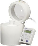
Rinser Dryer
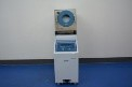
Make & Model: Verteq 8000
Automatic wafer cleaning with DI and spin drying with nitrogen.
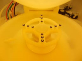
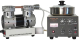
CPD
Make & Model: Tousimis Automegtadis
- Process up to 6" (150mm) wafers, Automatic Supercritical Point Dryer
- wafer holders and inserts are provided that allow anti-stiction processing up to 5 pieces of either 6" (150mm), 4" (100mm), 3" (75mm), 2" (50mm) wafers or 10mm square die per process run